

From 4V to 400V: Building a High-Gain Boost Converter
⚠️ Disclaimer: This project involves high voltages (up to 400V). Mishandling can result in serious injury or death. Do not replicate this unless you understand the risks and follow strict safety precautions.
With my previous post as backdrop, this post explores the theory and technical challenges encountered when designing the DC-DC boost converter used in our rocket igniter a few years back.
In this post, you will find:
- An introduction to how a DC-DC boost converter works
- An overview of two well-known models for DC-DC boost converters
- Why the common models do not apply in this case → Time to build a custom model
- A real DC-DC boost converter circuit and a comparison with the derived model
While designing a basic boost converter isn’t difficult, pushing it to deliver high voltage gain and fast power transfer brings a new level of complexity—especially when learning everything from scratch and without prior academic or professional experience in power electronics.
Introduction
As the name suggests, a DC-DC boost converter raises a DC input voltage to a higher DC output voltage. The core circuit is simple, typically involving just an inductor, diode, capacitor, and a switch (usually a transistor).
The animation below shows the general behaviour of such a circuit. If it seems confusing at first glance, feel free to revisit it later as you read.
How does it work?
One key trick to understanding how this circuit works is to break it into two phases, depending on whether the switch is closed or open.
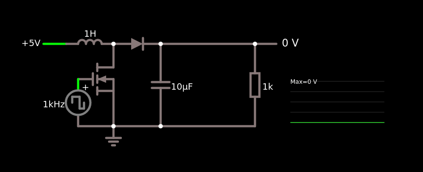
These two phases correspond to the following simplified ideal circuits:
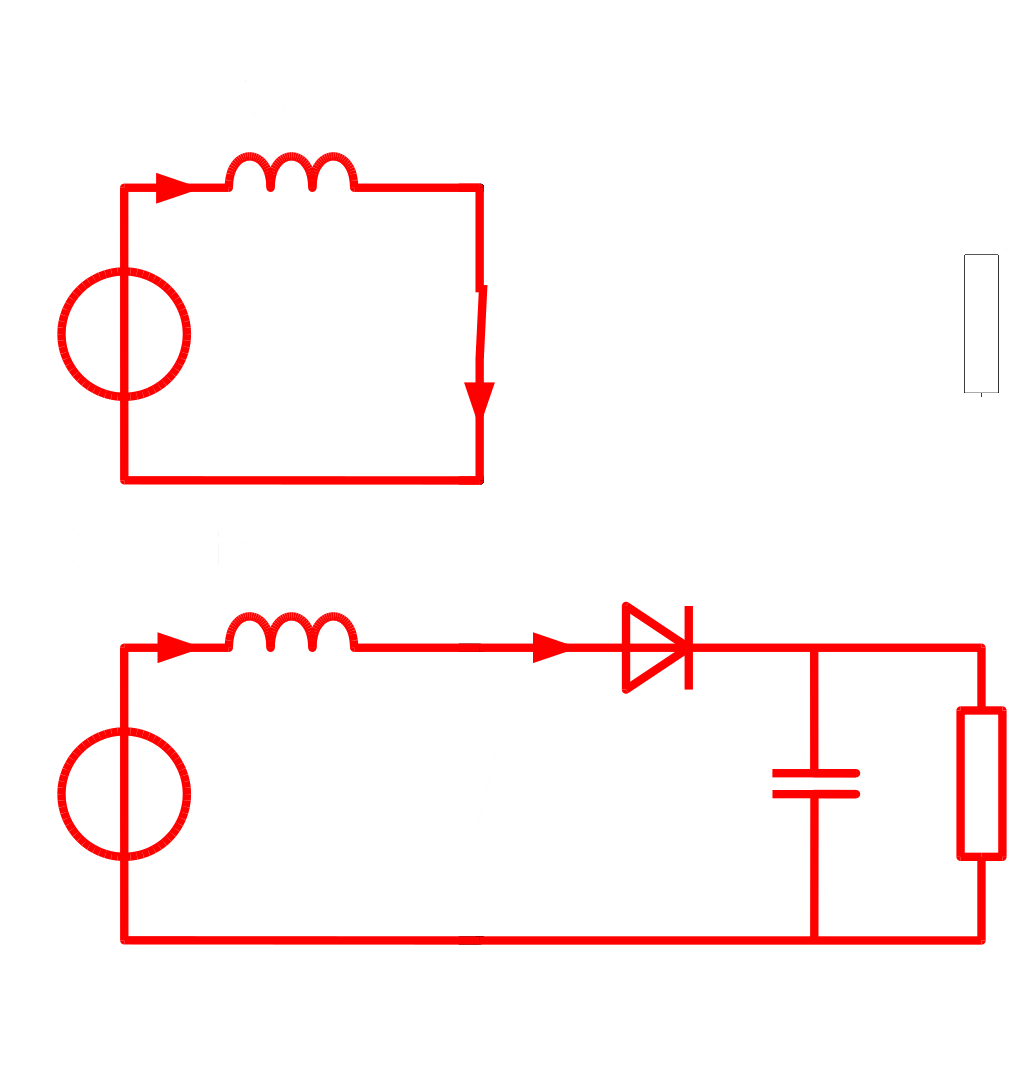
Of course, these are ideal models. In real circuits, parasitic resistances in the inductor, battery, and wires have a significant effect. Still, these two basic phases help grasp the core operating principle.
Switch Closed. Charge Phase
- The switch (transistor) conducts, closing the upper loop.
- The inductor initially has no current: $I=0$ at $t=0$.
- Current ramps up through the inductor, storing energy in its magnetic field.
- Ideally, just before saturation or reaching a target current, the switch opens.
Switch Open. Discharge Phase
- The switch just opened, forming a new loop through the diode and capacitor.
- The inductor, now “charged,” resists sudden current change and keeps current flowing.
- This energy is transferred to the capacitor, increasing its voltage $V_0\rightarrow V_0+\Delta V$.
- Repeating this cycle steadily increases the capacitor’s voltage.
Theory overview
Most boost converters are designed for steady-state operation with a continuous load, such as powering a 12V device from a 5V USB source. In this steady regime, current through the inductor does not fall to zero and switching is done in such a way as to stay within the linear range of the inductor.
Although the mentioned continuous mode with linear current derivative in the inductor is the most common, the analysis can be considered in some other ways:
- Continuous mode. The mentioned "Standard" Model.
- The inductor charges linearly when the switch is closed.
- It discharges linearly to the load and capacitor when the switch opens. Still, the current through the inductor never reaches zero.
- Easy to model and very efficient.
- The relation between the output voltage $V_o$ and the input voltage $V_i$ depends solely on the duty cycle of the switching $D$. So, the expression is just $$\frac{V_o}{V_i}=\frac{1}{1-D}$$
- Discontinuous mode.
- Charging phase is similar to the continuous, but starting from zero current.
- Discharge is quicker due to a low-resistance load. In this case the current does reach zero, therefore the name "discontinuous mode".
- More complex to model and efficiency usually drops, compared with continuous mode.
- The gain is more complex, being $$\frac{V_o}{V_i}=\frac{1}{2}\left(1+\sqrt{1+\frac{2D^2RT}{L}}\right)$$ Where $R$ is the load resistance, $L$ is the inductance of the coil and $T$ is the commutation period.
- "Fast-discharge, unsteady" Discontinuous mode. I have not seen this in books, so I made up the name.
- The inductor charges similarly to the previous cases.
- There’s essentially no load, only a capacitor. The current does drop to zero and the discharge phase is very fast. Somewhat similar to the discharge at the discontinuous mode.
- $\frac{V_o}{V_i}\rightarrow \infty$ when $t\rightarrow \infty$ and energy efficiency is lower than the other modes.
The fast-discharge, unsteady discontinuous mode, could represent the power up of any DC-DC Boost Converter. The transient phase before the steady operation mode. The goal this time is very different from the, steady, fixed gain in the other modes. The goal is to ramp up the voltage as fast and high as possible, without a steady state and without a main focus on energy efficiency.
Fast-discharge, unsteady discontinuous mode model
Since, I could not find a model that describes this, deriving a simple one is the main purpose of this section. The model is intended to provide–ideally quantitative– information about the fastest possible charge of the output capacitor. Each "step" or cycle of the charging process is divided in a charging phase and a discharging phase of the inductor. These two will be analysed individually and combined towards the end, to conform a full view of the system.
Charge expected time
The charging loop closes a RL circuit. The current is known to follow the exponential behaviour
$$I\left(t\right)=\frac{V}{R}\left(1-e^{-t/\tau}\right)\qquad\tau=\frac{L}{R}$$
$\tau$ is the characteristic time constant. It represents the time required for the current to increase or decrease by a factor of $e=2.718...$. $R$ is the equivalent series resistance of the charging loop, $V$ is the voltage of the battery and $L$ is the inductance of the inductor. The charging time will be of the order of magnitude of the time constant
$$\boxed{t_{\mathrm{c}}^{\mathrm{RL}}\approx K\tau=K\frac{L}{R_{\mathrm{c}}}}$$
where the subindex $\mathrm{c}$ stands for ‘charge’ and $K\in\left(0,5\right)$, since the charging time will be less than $5\tau$. As usual, $5\tau$ is chosen to be the time for a ‘full’ charge — it would be infinite otherwise. Note that the resistance during charging differs from that during discharge, hence the use of a subscript from now on.
Discharge expected time
The discharge loop forms an RLC circuit, which is inherently more complex. An RLC circuit can exhibit three different types of behaviour, determined by the damping factor $\alpha=\frac{R}{2L}$ and the natural (resonant) frequency $\omega_{0}=\frac{1}{\sqrt{LC}}$. These two parameters combine to define the damped angular frequency of the system:
$$\omega_{d}=\sqrt{\omega_{0}^{2}-\alpha^{2}}=\sqrt{\frac{1}{LC}-\left(\frac{R}{2L}\right)^{2}}$$
These frequencies determine the behaviour of the circuit. In our circuit,
$$C=1880\cdot10^{-6}\;\mathrm{F}\qquad L=10^{-4}\;\mathrm{H}\qquad R_{\mathrm{d}}=0.118\;\mathrm{\Omega}$$
meaning that
$$\alpha=\frac{R_{\mathrm{d}}}{2L}\approx590\qquad\omega_{0}=\frac{1}{\sqrt{LC}}\approx2306$$
This means the system operates in the underdamped regime, since $\omega_{0}>\alpha$. In this case, the voltage follows a damped sinusoidal response, governed by an equation of the form:
$$V\left(t\right)=e^{-\alpha t}\left[A\cos\left(\omega_{d}t\right)+B\sin\left(\omega_{d}t\right)\right]$$
By applying the boundary conditions $I\left(t=t_{f}\right)=0$, $I\left(t=0\right)=I_{0}$, $V\left(t=t_{f}\right)=V_{f}$ and $V\left(t=0\right)=V_{0}$, plus the current equation, one can find the value of $A$ and $B$. $A$ is quite straightforward
$$V\left(t=0\right)=V_{0}=A$$
For $B$, the current equation has to be used
$$I\left(t\right)=C\frac{dV\left(t\right)}{dt}=-\alpha Ce^{-\alpha t}\left[A\cos\left(\omega_{d}t\right)+B\sin\left(\omega_{d}t\right)\right]+Ce^{-\alpha t}\left[-A\omega_{d}\sin\left(\omega_{d}t\right)+B\omega_{d}\cos\left(\omega_{d}t\right)\right]=$$
$$=Ce^{-\alpha t}\left[-A\alpha\cos\left(\omega_{d}t\right)-B\alpha\sin\left(\omega_{d}t\right)-A\omega_{d}\sin\left(\omega_{d}t\right)+B\omega_{d}\cos\left(\omega_{d}t\right)\right]$$
If $I\left(t=0\right)=I_{0}$, the trigonometric functions reduce to either zero or one, so it is simplified to
$$I_{0}=C\left(-A\alpha+B\omega_{d}\right)$$
All the above results in the final values for $A$ and $B$
$$\boxed{A=V_{0}\qquad B=\frac{\frac{I_{0}}{C}+\alpha V_{0}}{\omega_{d}}}$$
Now, with the current equation and the values of $A$ and $B$, the discharge time can be easily found by setting the current to zero — marking the end of the discharge. Since the solution is underdamped, energy would normally oscillate between the capacitor and the inductor. However, in a DC-DC boost converter, the diode prevents current reversal by interrupting the flow as soon as it attempts to go backward. This behaviour is advantageous: the current reaches zero earlier than in critically or overdamped cases — as a natural consequence of the underdamped solution — while still avoiding oscillations. Let’s find the discharge time by solving $I\left(t_{\mathrm{d}}\right)=0$, where $\mathrm{d}$ stands for the discharge time.
$$0=e^{-\alpha t_{\mathrm{d}}}\left[-A\alpha\cos\left(\omega_{d}t_{\mathrm{d}}\right)-B\alpha\sin\left(\omega_{d}t_{\mathrm{d}}\right)-A\omega_{d}\sin\left(\omega_{d}t_{\mathrm{d}}\right)+B\omega_{d}\cos\left(\omega_{d}t_{\mathrm{d}}\right)\right]\implies$$
Discarding the trivial case when $e^{-\alpha t_{\mathrm{d}}}\rightarrow0$, $t_{d}\rightarrow\infty$
$$0=-A\alpha\cos\left(\omega_{d}t_{\mathrm{d}}\right)-B\alpha\sin\left(\omega_{d}t_{\mathrm{d}}\right)-A\omega_{d}\sin\left(\omega_{d}t_{\mathrm{d}}\right)+B\omega_{d}\cos\left(\omega_{d}t_{\mathrm{d}}\right)$$
$$\left(B\alpha+A\omega_{d}\right)\sin\left(\omega_{d}t_{\mathrm{d}}\right)=\left(B\omega_{d}-A\alpha\right)\cos\left(\omega_{d}t_{\mathrm{d}}\right)$$
$$\tan\left(\omega_{d}t_{\mathrm{d}}\right)=\frac{B\omega_{d}-A\alpha}{B\alpha+A\omega_{d}}=\frac{\omega_{d}I_{0}}{\alpha I_{0}+CV_{0}\left(\alpha^{2}+\omega_{d}^{2}\right)}$$
We found that
$$\boxed{t_{\mathrm{d}}^{\mathrm{RLC}}=\frac{1}{\omega_{d}}\arctan\left(\frac{\omega_{d}I_{0}}{\alpha I_{0}+C\omega_{0}^{2}V_{0}}\right)}$$
$\omega_{d}$, $\alpha$ and $C$ are constants dependent on the circuit components, and $I_{0}$ will be the maximum current achieved by the RL circuit, as enforced by the continuity of the current
$$\boxed{I_{0}=\frac{V_{\mathrm{bat}}}{R_{\mathrm{c}}}\left[1-e^{-K}\right]}$$
That is a constant throughout all the charging process, that will be fixed when choosing $K$. The only real variable is $V_{0}$, that will depend on the previous state of the capacitor at the end of the previous cycle.
Optimal frequency and duty cycle
The expression for the frequency and duty cycle are easily found from their definitions. The frequency will be the inverse of the period, that is given by the total cycle time.
$$T=t_{\mathrm{c}}^{\mathrm{RL}}+t_{\mathrm{d}}^{\mathrm{RLC}}=K\frac{L}{R_{\mathrm{c}}}+\frac{1}{\omega_{d}}\arctan\left(\frac{\omega_{d}I_{0}}{\alpha I_{0}+C\omega_{0}^{2}V_{0}}\right)$$
$$f=\frac{1}{T}=\frac{1}{K\frac{L}{R_{\mathrm{c}}}+\frac{1}{\omega_{d}}\arctan\left(\frac{\omega_{d}I_{0}}{\alpha I_{0}+C\omega_{0}^{2}V_{0}}\right)}$$
The duty cycle is given by the time spent with the NMOS conducting within the full cycle
$$D=\frac{t_{\mathrm{c}}^{\mathrm{RL}}}{t_{\mathrm{c}}^{\mathrm{RL}}+t_{\mathrm{d}}^{\mathrm{RLC}}}=\frac{K\frac{L}{R_{\mathrm{c}}}}{K\frac{L}{R_{\mathrm{c}}}+\frac{1}{\omega_{d}}\arctan\left(\frac{\omega_{d}I_{0}}{\alpha I_{0}+C\omega_{0}^{2}V_{0}}\right)}$$
Note that the only unknown is $K$, which represents the control we have over the charging phase. The discharge time is fixed, but the charging can be stopped at will by turning off the NMOS transistor. What is the optimal value of $K$ for the fastest charging process?
Intuitively, this value should be far from the saturation region, yet still allow a high current. A high current is desirable, since the stored energy increases quadratically with it. However, saturation should be avoided: in the saturation region, the current through the inductor no longer increases significantly with time, meaning that the energy will no longer grow appreciably either.
A valid perspective is to maximise the output power relative to the maximum power the battery can theoretically deliver. This can be formalised as maximising the following function:
$$\frac{E_{\mathrm{L}}^{\mathrm{cycle}}\left(K\right)}{P_{\mathrm{Bat}}t_{\mathrm{c}}^{\mathrm{LR}}\left(K\right)}=\frac{\frac{1}{2}L\overbrace{\left[\frac{V_{\mathrm{bat}}}{R_{\mathrm{c}}}\left(1-e^{-K}\right)\right]^{2}}^{\left[I\left(K\right)\right]^{2}}}{\frac{V_{\mathrm{Bat}}^{2}}{R_{\mathrm{Bat}}}\cdot K\frac{L}{R_{\mathrm{c}}}}=\frac{R_{\mathrm{Bat}}}{R_{\mathrm{c}}}\cdot\frac{\left(1-e^{-K}\right)^{2}}{2K}$$
$$\boxed{\eta_{\mathrm{Power}}\equiv\frac{E_{\mathrm{L}}^{\mathrm{cycle}}\left(K\right)}{P_{\mathrm{Bat}}t_{\mathrm{c}}^{\mathrm{LR}}\left(K\right)}=\frac{R_{\mathrm{Bat}}}{R_{\mathrm{c}}}\cdot\frac{\left(1-e^{-K}\right)^{2}}{2K}}$$
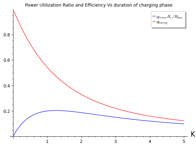
This is known as the Power Utilization Ratio. In addition, the standard definition of energy efficiency is the energy stored in the coil per cycle divided by the energy supplied by the battery during that same period
$$\frac{E_{\mathrm{L}}^{\mathrm{cycle}}\left(K\right)}{P_{\mathrm{Bat}}t_{\mathrm{c}}^{\mathrm{LR}}\left(K\right)}=\frac{\frac{1}{2}L\left[\frac{V_{\mathrm{bat}}}{R_{\mathrm{c}}}\left(1-e^{-K}\right)\right]^{2}}{\int_{0}^{t}V_{\mathrm{bat}}\underbrace{\frac{V_{\mathrm{bat}}}{R_{\mathrm{c}}}\left(1-e^{-K}\right)}_{I\left(K\right)}dt}=\frac{\cancel{L\frac{V_{\mathrm{bat}}}{R_{\mathrm{c}}}}\left(1-e^{-K}\right)^{2}}{2\cancel{L\frac{V_{\mathrm{bat}}^{2}}{R_{\mathrm{c}}^{2}}}\int_{0}^{K}\left(1-e^{-K}\right)dK}$$
$$\boxed{\eta_{\mathrm{Energy}}\equiv\frac{E_{\mathrm{L}}^{\mathrm{cycle}}\left(K\right)}{P_{\mathrm{Bat}}t_{\mathrm{c}}^{\mathrm{LR}}\left(K\right)}=\frac{1}{2}\frac{\left(1-e^{-K}\right)^{2}}{K+e^{-K}-1}}$$
where the substitution $dt=\frac{L}{R_{\mathrm{c}}}dK$ has been used, since $t=K\frac{L}{R_{\mathrm{c}}}$. I apologise for the abuse of notation in using $K$ to denote both the variable and the integration parameter.
It is useful to get some visual insight with a couple of graphs. The first graph shows the power utilization ratio, while the second shows both, the power utilization ratio (adimensional: $\eta_{\mathrm{Power}}\frac{R_{\mathrm{c}}}{R_{\mathrm{Bat}}}$) and the efficiency.
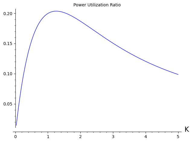
The optimal value of $K$ is the solution to
$$\frac{d}{dK}\left(\frac{E_{\mathrm{L}}^{\mathrm{cycle}}\left(K\right)}{P_{\mathrm{Bat}}t_{\mathrm{c}}^{\mathrm{RL}}\left(K\right)}\right)=0$$
This answers the key question: when should charging be stopped to extract the maximum energy per converter cycle? Consequently, what is the fastest charge? Since we live in the 21st century, I won’t solve this by hand, but numerically with SageMath. For my circuit parameters, this yields:
$$\boxed{K\approx1.26}$$
This means the fastest charge is achieved when the inductor is charged for approximately $1.26\cdot L/R_{\mathrm{c}}$ seconds. With this, the previously open problem is resolved, and both the optimal frequency and duty cycle of the converter are fully defined.
Optimal frequency and duty cycle for maximum power output
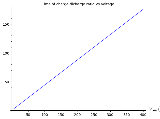
All the equations are determined and the frequency and duty cycle can be computed. There is only one catch to it: they depend on the output capacitor's voltage. Let's have a look at the different plots with the voltage:
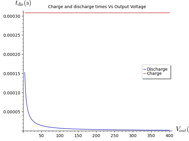
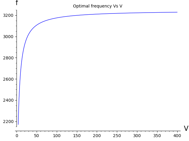
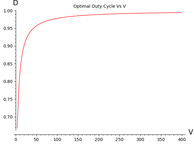
As can be seen, both the frequency and duty cycle eventually reach a plateau where their values remain nearly constant. Moreover, since energy increases quadratically with voltage, this plateau is achieved very quickly. This suggests that, rather than dynamically tracking the exact curves, selecting the constant value corresponding to the plateau is nearly just as effective — and significantly simpler to implement. The following graph shows the percentage of energy as a function of the voltage.
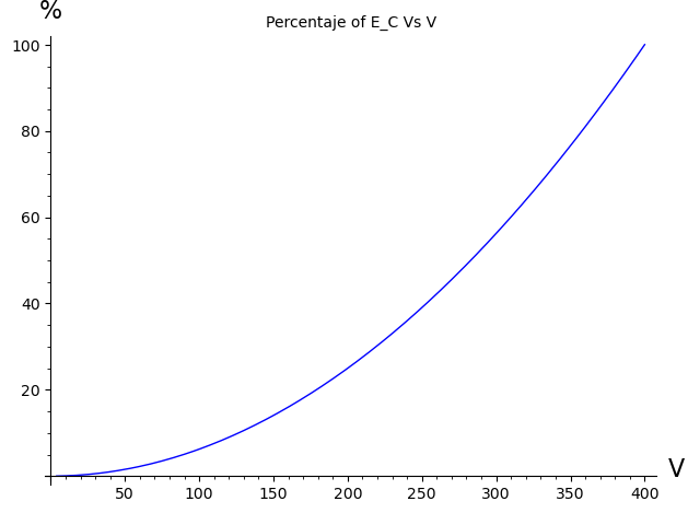
In line with this reasoning, the firmware will use fixed values for frequency and duty cycle, chosen to correspond to the point at which the inductor has accumulated half of its maximum cycle energy. This is, when
$$V_{o} = 200\sqrt{2}$$
Factors not included in the model
One finds that there are several additional relevant factors not considered in this model:
- Switching: The switching time of the transistor and the recovery time of the diode take up a small fraction of the charging and discharging cycles. It is recommended to use ultra-fast switching NMOS transistors and diodes. To avoid including these, high-frequencies are avoided when choosing the components.
- Temperature: If heat is not properly dissipated, it can lead to high component temperatures, which increase resistance and alter behaviour. This can cause the optimal operating frequency to shift slightly during operation. If the circuit avoids unnecessary time of short circuit in the charge, this is not that relevant.
- Maximum gain: The maximum achievable gain of the circuit occurs when the leakage current of the capacitor matches the energy supplied by the boost converter. So it is not actually infinite.
- Maximum Ratings. Electronic components have physical limits for current, voltage, power dissipation... The model will not work outside of those boundaries. Additionally, unsuspected phenomena can happen. For example, the inductor can start arching internally if the output voltage is too high for the isolation between coil loops.
- NMOS gate delay. The gate is driven by a ~18 signal from a Dickson charge pump. Due to the presence of resistance, the gate’s capacitance forms an RC circuit, which introduces a delay when driving high or low the gate. This results in the NMOS presenting a higher resistance for a brief period during the cycles.
The actual circuit
Circuit Overview
The circuit consists of three main stages: the Powering Stage, the DC-DC Boost Converter, and the Discharge Stage. In addition, a simple control logic circuit manages the operation of the main system. These parts are highlighted in the schematic.
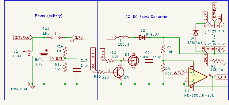
- Powering Stage. This stage includes a latching push button used to (dis)connect the high-current 3.7V LiPo battery, as well as a voltage divider that provides a measurement point for monitoring the battery level. There are two 3.7V lines: one powers the low-voltage logic, while the other — labelled
3.7VRAW— bypasses the button and supplies the Boost Converter directly. This design avoids the need for a high-current-rated push button, which would be bulky and expensive. - DC-DC Boost Converter Stage. This stage includes the inductor, an ultra-fast recovery diode, the output capacitor, and the NMOS transistor that performs the switching. The
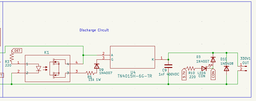
V++signal connected to the NMOS gate is at a higher voltage than the control logic, allowing the NMOS to conduct more efficiently. Another transistor,Q3, is a BJT controlled by the oscillator in the logic circuit; it drives the NMOS gate at the desired switching frequency. A voltage divider is also included in this stage to monitor the output voltage, enabling the system to stop charging when the target voltage is reached. An operational amplifier is used as a buffer to isolate the divider’s impedance from the control logic, preventing measurement errors due to loading effects. In the upper right corner, there is a relay. Its function is to physically disconnect the Boost Converter from the discharge circuit before the discharge occurs – or when powered off–. Additionally, it connects the output capacitor to a 22 kΩ, 4 W discharge resistor labelledDISCHwhen not charging. This ensures the high voltage is safely discharged in case something goes wrong. The circuit is therefore designed to charge and immediately trigger the high-voltage discharge, avoiding having a charged high-voltage capacitor sitting idle. - Discharge Stage. This section is designed to safely switch the discharge and to isolate, as much as possible, both the low-voltage logic and the Boost Converter from the high-voltage, high-current discharge path. The switching is controlled through
K1, an optocoupler. It drives the main switching device,U4, which is an SCR (Silicon Controlled Rectifier) that performs the actual discharge. The 15 kΩ resistor connected to the gate of the SCR is intended to provide a small current just above the triggering threshold, allowing the SCR to enter conduction mode. By sourcing this current from the output capacitor’s voltage, the triggering becomes largely independent of the external load at the output—as long as that load remains within the intended range (from approximately 0 Ω to ∼2 kΩ). The capacitor placed right after the optocoupler ensures that enough gate charge is delivered to the SCR to trigger conduction reliably. The LED and protection diodeD3conduct whenever the output loop is closed — that is, when a load is connected. If the output is open, the LED remains off, serving as an indicator. The final diode,D10, is a flyback diode that protects the circuit against reverse voltage spikes in case the discharge load is inductive. - Low-Voltage Control Logic. The control logic can be fully analog or implemented with a microcontroller. The first version of the circuit used an astable multivibrator and operational amplifiers configured as comparators to stop the charge at a given voltage. However, this setup was later replaced by a PIC16 microcontroller and eventually by an ESP32-C3. The
V++signal applied to the NMOS gate is generated using a simple Dickson charge pump, as the output power required is very low.
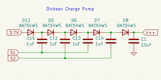
S1 and S2 are two PWM signals shifted 180º out of phase.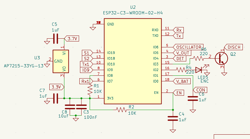
S1 and S2 control the charge pump. V_OUT provides samples of the output voltage level. DISCH switches between the charge path and the discharge circuit. V_BAT monitors the battery voltage. CON detects whether the discharge load is connected. DET enables the SCR to conduct, triggering the high-power discharge at the output. The rest includes the UART programming interface and an additional UART interface for communication with other microcontrollers if needed.PCB Design Considerations
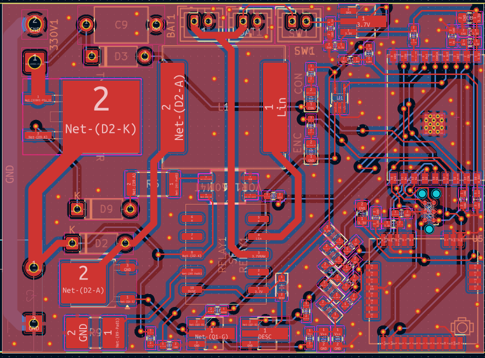
PCB design rules are the same as any other PCB for the low voltage components. For the high-power components, there are some additional effects to consider:
- Low resistance traces. Use wide traces and expose them for further reinforcement with solder or external wire.
- Proper spacing. Keep enough spacing between traces and components, to avoid electric arcs with high-voltage spikes.
- Magnetic field. High-current will induce currents in nearby traces through the induced magnetic field. Space them properly and try to avoid parallel traces to minimize the effect.
- Proper grounding. Ensure all the ground connections are good enough to dissipate a strong current without melting. Same goes for any critical part of the circuit with higher resistance than the rest of the loop.
- Thermal dissipation. Keep in mind that some components might get very hot during prolonged charging periods, so make sure they can dissipate their heat fast enough through the PCB ground plane or external heat sinks.
To put numbers to those categories, one can make some rough estimates, run a simulation or check recommended values online. In any case, carry out the testing with safety in mind and take care.
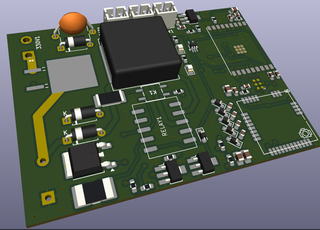
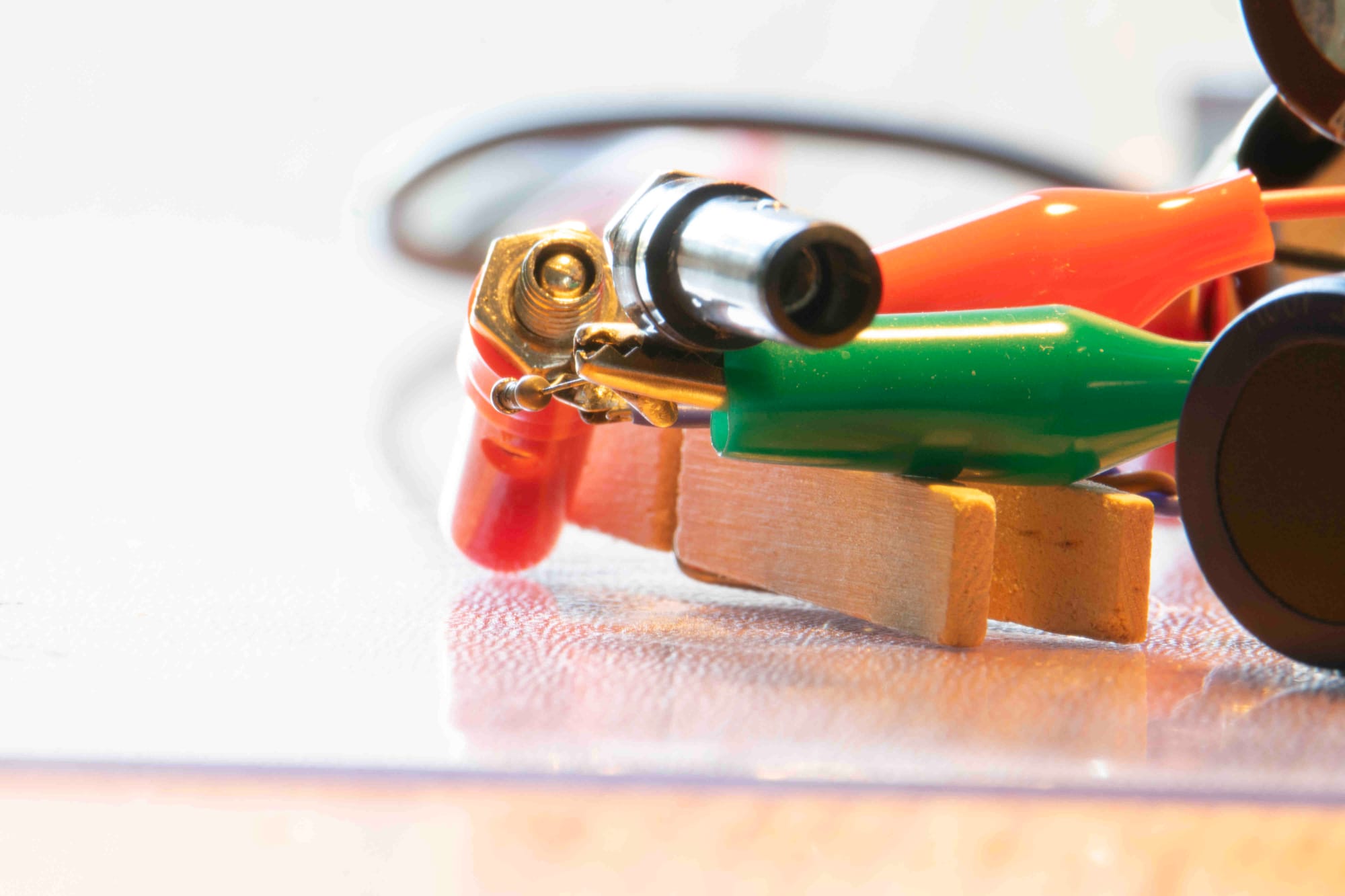
The Physical Circuit
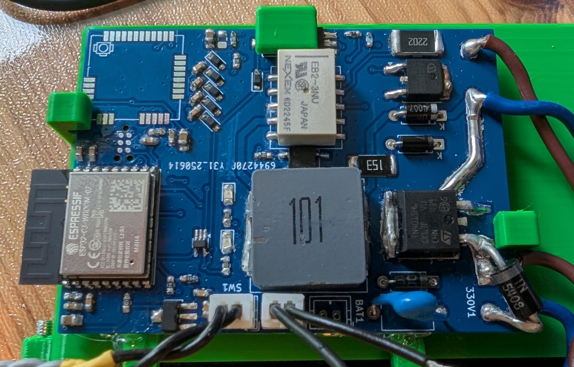
As I revisit this project, the PCB is being repurposed for a different use than originally intended. Instead of functioning as a rocket igniter, it will now be used to charge a capacitor bank and fire a small, portable coilgun — a project that will be the focus of the next post. In this new context, including the radio module no longer makes sense, so it has been left out.
In the past, I spent many hours probing signals in this circuit. However, as often happens when things aren’t documented, much of that work has been lost over time. This meaning that, to spare time, less measurements than I would like are going to be presented.
First, I present some component values and the corresponding model parameters. Some measurements and pictures will follow, contrasting with the predictions of the model. Therefore, the relevant circuit parameters are
$$L = 100\cdot 10^{-6}\;\mathrm{H}\quad C = 1880\cdot 10^{-6}\;\mathrm{F}\quad V_{\mathrm{Bat}} = 4\;\mathrm{V}$$
$$R_{\mathrm{Bat}} = 0.140\;\mathrm{\Omega}\quad R_L = 0.118\;\mathrm{\Omega}\quad R_\mathrm{Tran} = 0.30/2=0.15\;\mathrm{\Omega}$$
These correspond, respectively, to the inductance of the coil, the capacitance of the output capacitor(s), the battery voltage, the internal resistance of the battery, the resistance of the coil, and the on-resistance of the NMOS transistor. The latter is divided by two because a second NMOS was soldered in parallel to reduce resistance. While not strictly necessary, this becomes more relevant in the coilgun context, where charging times are significantly longer.
From these values, the equivalent series resistances during the charge and discharge phases are:
$$R^{\mathrm{RL}}_{\mathrm{c}}=0.408\;\mathrm{\Omega} \qquad R^{\mathrm{RLC}}_{\mathrm{d}}=0.118\;\mathrm{\Omega}$$
Using all these parameters and the expressions for optimal frequency and duty cycle, we obtain
$$f\left(V_{o} = 200\sqrt{2}\right)=\frac{1}{K\frac{L}{R_{\mathrm{c}}}+\frac{1}{\omega_{d}}\arctan\left(\frac{\omega_{d}I_{0}}{\alpha I_{0}+C\omega_{0}^{2}V_{0}}\right)}\approx 3221\;\mathrm{Hz}$$
$$D\left(V_{o} = 200\sqrt{2}\right)=\frac{K\frac{L}{R_{\mathrm{c}}}}{K\frac{L}{R_{\mathrm{c}}}+\frac{1}{\omega_{d}}\arctan\left(\frac{\omega_{d}I_{0}}{\alpha I_{0}+C\omega_{0}^{2}V_{0}}\right)}\approx 99.2\%$$
Technically, both values depend on the output voltage, but it is assumed to remain approximately constant for most of the charge cycle. The voltage used here corresponds to the value at which the capacitor has reached 50% of its maximum energy — as discussed earlier.
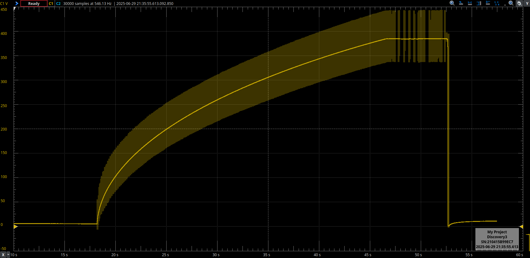
With the circuit operating at the calculated frequency and duty cycle, it’s time to take some measurements. The first one — since it’s very easy to obtain — is the time required to fully charge the capacitors. A small Python script is used to emulate all the charge/discharge cycles and sum their durations. In the real circuit, a full charge is timed manually using a stopwatch. The results are:
$$t_{\text{Full charge}}^{\text{Theory}} \approx 18.1\;\mathrm{s}$$
$$t_{\text{Full charge}}^{\text{Measured}} \approx 27.5\;\mathrm{s}$$
Although the result is not highly accurate — with a relative error of about 50% — the order of magnitude matches. This suggests that the model is conceptually solid, though it lacks the refinement necessary for precise predictions. Additionally, the theoretical time is shorter than the measured one, which is expected, as the model does not account for energy losses and other non-ideal effects.
Interestingly, when powering the circuit from my lab power supply, I can monitor the instantaneous current being drawn. It shows a slight increase during the first half of the capacitor bank charging process, followed by a gentle decrease as the charge progresses. This behaviour aligns well with the choice of optimal frequency and duty cycle based on the voltage corresponding to 50% of the total stored energy. Observing this effect — just as predicted by the model — was quite encouraging.
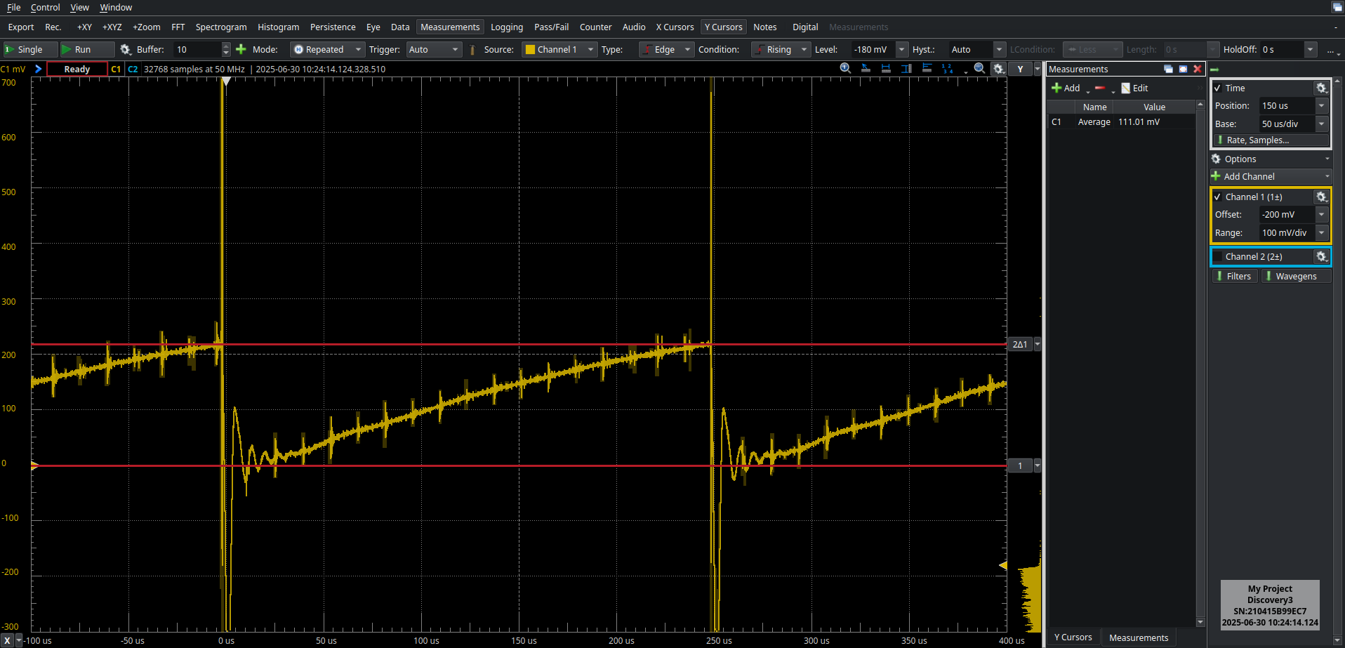
While the predicted frequency and duty cycle are unlikely to be truly optimal, they are clearly in the right track. I tested a range of frequencies from 1 kHz to 10 kHz, and in both directions the capacitor bank charging time increased significantly. The low-frequency end is particularly problematic: the charging cycles push the inductor into saturation, effectively turning the converter into a short circuit during those intervals. This results in excessive heating and increased resistance. At the 10 kHz end, the system is safer — the peak current per cycle is lower, leading to minimal heating — but the reduced energy transfer per cycle makes the charging slower.
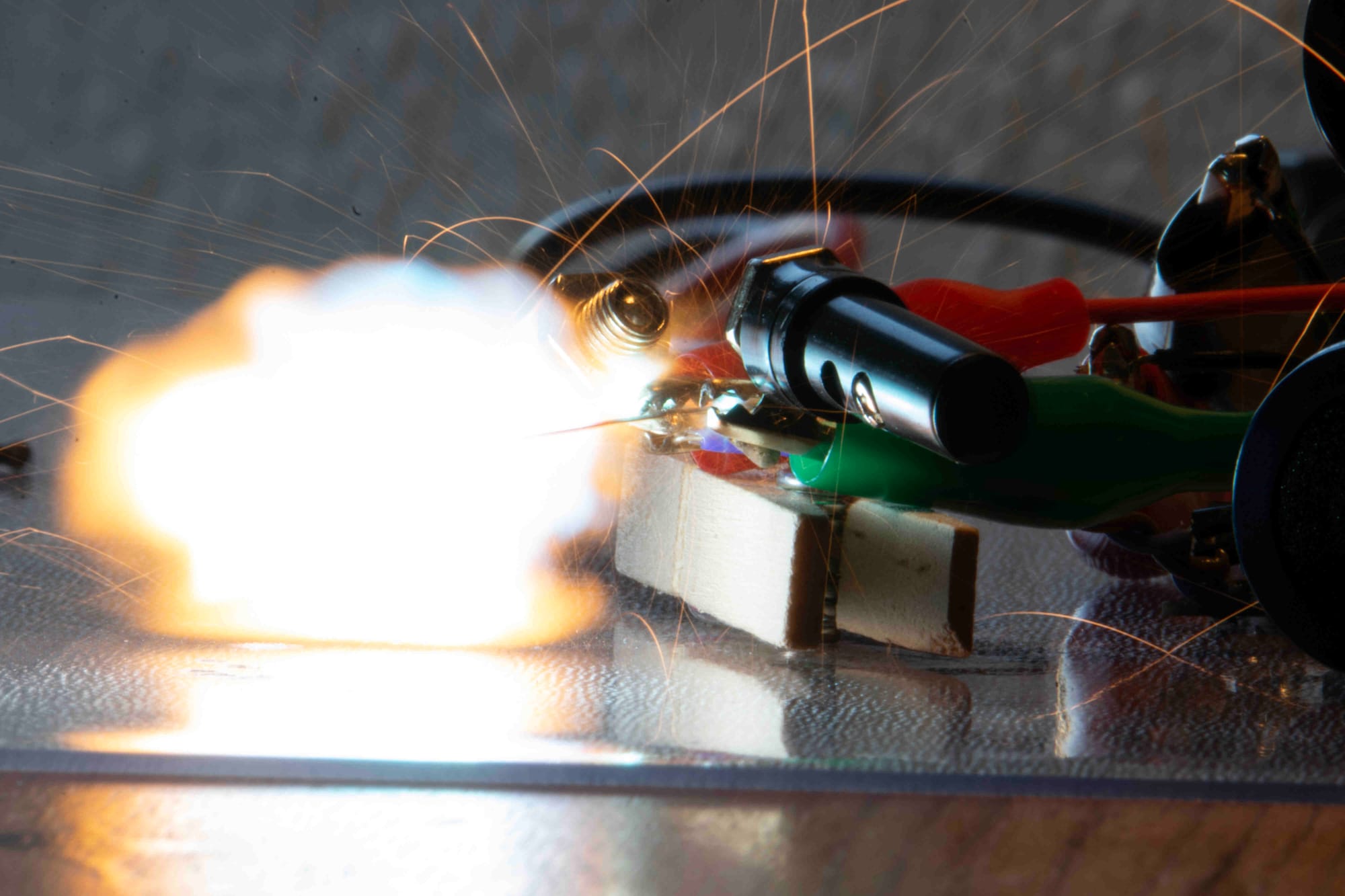
In the following section, I include several graphs and images related to the measurements and discharge behaviour of the circuit. For these experiments, the operating frequency was shifted from the previously determined optimal point toward the higher-frequency range – to $4\;\mathrm{kHz}$. While this adjustment slightly increases the total charging time, it reduces the average current during the charge phases — which was, in average, exceeding the rated current of the relay used in the circuit.
Problems Encountered During Testing
The first time inexperienced hands test this kind of circuit, it can be a real nightmare. Here are some of the issues found, with possible solutions:
- Voltage spikes frying the microcontroller
High-voltage transients found their way back to the microcontroller, killing it instantly. The solution: place protection diodes in all possible paths and be extremely careful with PCB trace layout. - PCB traces vaporising during discharge
The traces connecting the capacitor to the output literally exploded — instantly and completely. Use very thick traces, and expose them so you can reinforce with solder if needed. - Internal arcing inside the inductor
When pushing to very high voltages, internal arcs formed inside the coil. Make sure your inductor is properly insulated for the voltages you plan to work with. - Relay contacts welding shut
If a relay switches while high current is still flowing, its terminals can weld together. Ensure the current is close to zero before toggling any relays. This is a risk within the charging loop or the final discharge from the capacitor. - Arcs forming during switching
When toggling a switch or relay, an arc can form as the contacts briefly get close. Test all mechanical switches to make sure they can handle the voltage, especially during switching. - Components overheating or smoking
At first, some components got extremely hot — even started to smoke. Start testing with higher PWM frequencies or lower duty cycles to avoid long shorts in the charging circuit. Monitor current carefully and be ready to unplug the power supply immediately. - Overloading the output capacitor
Sometimes the charge is very fast and can get to a higher voltage if not properly controlled by the microcontroller. Start testing with lower voltage limits, so you can stop the charge manually before it is too late.
Unfortunately, some of those are hard to predict without real-life testing, so be prepared for something to go wrong the first time you test the circuit. Always have proper monitoring of the circuit and some emergency shutdown control.
Conclusion and Circuit implementations
This post presented the design, modelling, and initial testing of a high-gain DC-DC boost converter. The theoretical model, though simplified, provided useful predictions that matched the circuit’s behaviour reasonably well, predicting correctly the order of magnitude of the charging time, and values of frequency and duty cycle close to the true optimal. Note that the measurements taken could be more accurate, possibly leading to values closer to those of the model predictions.
As a next step in the model's development, switching times, temperature effects, and parasitic elements could be included — likely resulting in a more accurate prediction. Additionally, directly measuring the component values would eliminate the effect of tolerances, which certainly impact the results.
The operating frequency was shifted slightly higher to reduce stress on components for normal operation. Additionally, since the circuit is being repurposed as a coilgun:
- The radio module was excluded.
- A second NMOS was soldered in parallel to minimise heating up.
- The output capacitor, originally $320\;\mathrm{\mu F}$ and $350\;\mathrm{V}$ was replaced by four $470\;\mathrm{\mu F}$ at $400\;\mathrm{V}$. It might seem overkill, but a coilgun is really inefficient...
The development of this circuit was initially motivated by inconsistent model rocket ignitions, but it gradually evolved to adapt to other uses as well. A few examples include:
- Reliable and safe model rocket ignition: It provides a reliable way to release the initial spark; precise in both time and location.
- Parachute ejection system: It can trigger the ejection charge of a rocket's parachute. The remote control feature also allows for a backup ignition signal in case the automatic system fails.
- Powering a small coil gun: I’ll soon present a project featuring a compact coil gun powered by this same circuit. Instead of triggering a spark, the discharge flows through a coil, generating a short but intense magnetic field.
- Circuit testing: With a few modifications, the circuit can serve as a high-voltage power source—either to energize other circuits or to test protection stages by releasing controlled discharges at different voltages.
In short, a circuit that is inherently dangerous by nature can actually enhance safety in scenarios like the ones above—if used with deep understanding, proper precautions, and extensive testing.
I hope you found the post interesting and informative. If you're planning to develop something similar, please think carefully before acting. Make sure you understand the risks involved, how the circuit works, and the necessary safety precautions.
